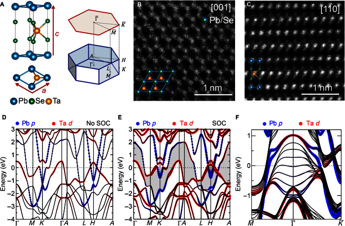
Fig. 1. Crystal structure and calculated band structure.
(A) Crystal structure of PbTaSe2 and the Brillouin zone of bulk (blue) and the Pb-terminated surface (red). (B) The HAADF image projected along the c axis, overlapped with a crystal structure signifying Ta (Pb/Se) atomic columns. (C) The HAADF image along the [110] projection, revealing the characteristic Pb monolayer and 1H-TaSe2 cages of PbTaSe2. Calculated band structure of PbTaSe2 (D) without SOC and (E) with SOC. The size of blue and red dots indicates the Pb p and Ta d orbital contributions, respectively. Large SOC splitting can be observed in Pb p and Ta d bands. The gray-shaded area indicates the continuous gap. (F) The decomposed surface band structure on the Pb-terminated surface of PbTaSe2 shows the projection of the Ta d and Pb p orbitals of the surface atoms. The gray circles indicate where the outer TSS merges into the bulk conduction bands.

