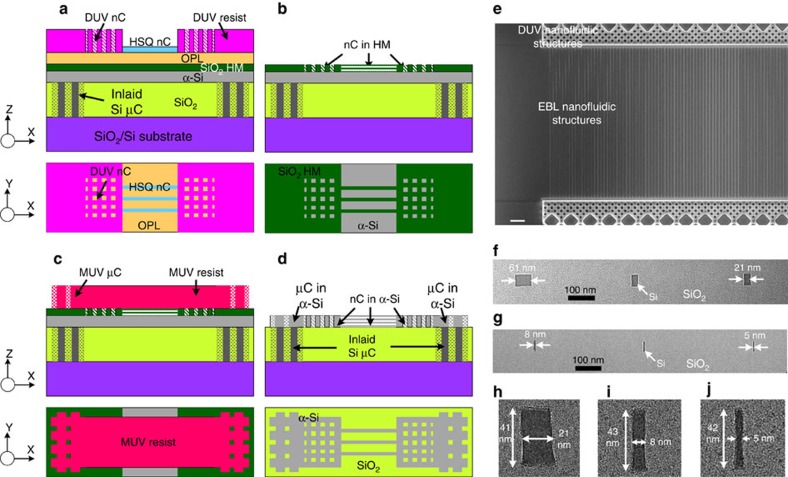
Figure 2. Three-level mixed lithography to fabricate Si sacrificial nanostructures.
(a–d) Fabrication scheme of patterning process (top: cross-sectional view in X–Z plane; bottom: top view in X–Y plane): (a) Combined nanopatterning of nanofluidic channel structures (nC) in deep ultraviolet (DUV) resist and EBL-defined hydrosilsesquioxane (HSQ) resist on an organic planarization layer (OPL)/SiO2 HM (hard mask)/α-Si film stack, with inlaid Si microchannels (μC) embedded and planarized in the substrate; (b) Nanofluidic structures transferred to HM layer; (c) MUV-patterned μC in resist; (d) α-Si fluidic structures with critical dimensions defined by MUV, DUV and EBL. (e-j) Fabricated nanofluidic structures: (e) Scanning electron microscope (SEM) image showing well-aligned DUV and EBL fabricated nanostructures before SiO2 capping; (f-j) Cross-sectional TEM images showing as small as <5 nm wide Si nanostructures in SiO2 capping layer. Scale bar in figure (e) is 2 μm.

