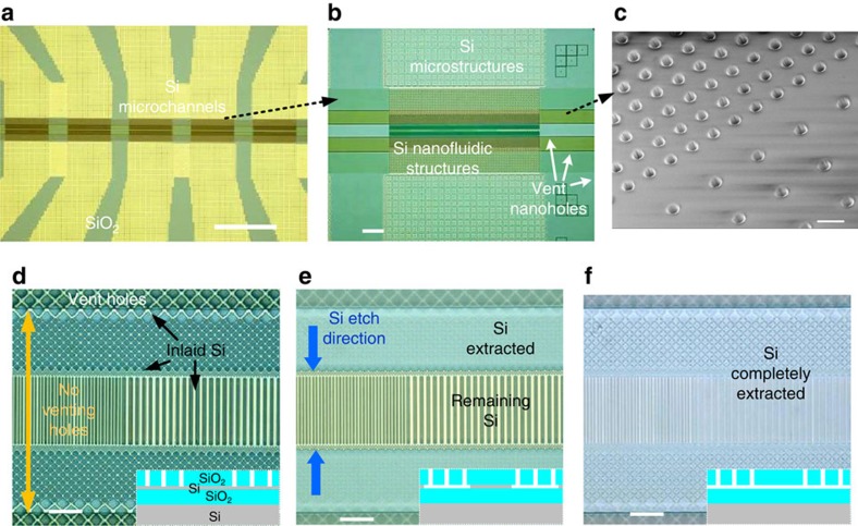
Figure 3. Sacrificial Si etching by XeF2.
(a,b) Optical images of fabricated sacrificial nanofluidic device prior to Si extraction, showing: (a) multiple fluidic branches on one chip; (b) Si microchannels connected by DUV-/EBL-fabricated Si structures in the middle. (c) 30° tilted SEM image of venting nanoholes in SiO2, with 300 nm diameters and different pitches (1 μm and 2 μm). (d–f) Optical images showing different stages of XeF2 etching: (d) before etching; (e) after partial Si extraction; (f) after complete Si extraction. The scale bars are 1 mm, 100 μm, 1 μm in figures (a–c), respectively, and 10 μm in d–f.

