Fig. 5.

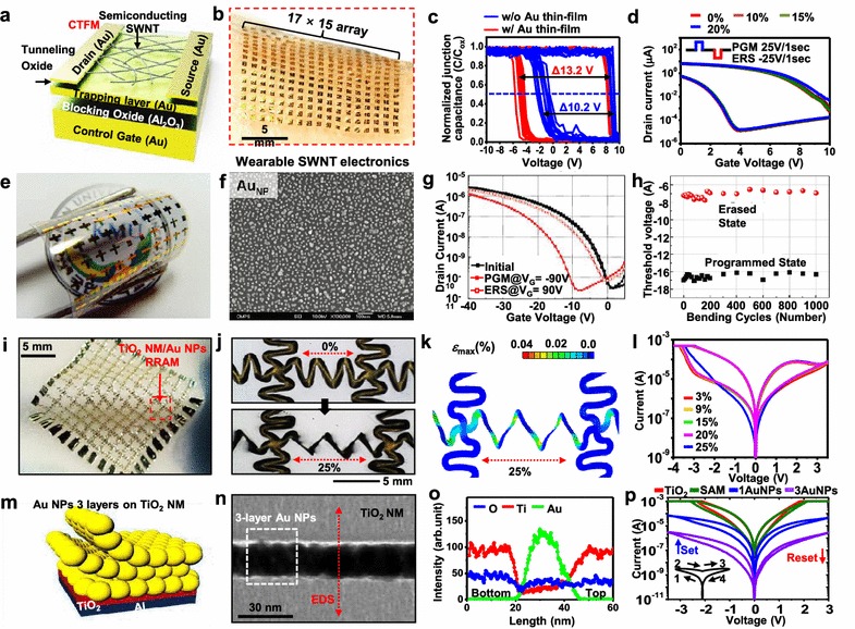
Nanomaterials embedded wearable memory devices. a Schematic of CTFM. b Photograph of the CTFM array conformally attached to human skin. c C–V hysteresis curves of a CNT-based memory capacitor with (red) and without (blue) an Au thin-film floating gate. d Transfer curves of stretched (0–20 %) CTFM for the program and erase modes. (a–d Reproduced with permission from Ref. [48], © 2015, American Chemical Society). e Photograph of a flexible organic memory device with an AuNP floating gate. f SEM image of AuNPs attached to the blocking oxide. g Transfer curves of the flexible organic memory device for the initial, programmed, and erased states. h Threshold voltage of the flexible organic memory device for the programmed and erased states according to the number of bending cycles. (e–h Reproduced with permission from Ref. [71], © 2010, American Chemical Society). i Photograph showing wearable RRAM attached to a medical bandage. j Optical images of wearable RRAM in the initial (top) and stretched (bottom) states. k Finite-element-analysis results showing the strain distribution of stretched (25 %) wearable RRAM. l I–V characteristic curves of wearable RRAM for different stretched states. m Schematic structural view of three layers of AuNPs assembled on a TiO2 nanomembrane, n TEM image showing three layers of AuNPs embedded between TiO2 nanomembranes. o Energy-dispersive X-ray spectroscopy results showing the quantitative material composition scanned along the red arrow in Fig. 5n. p I–V characteristic curves showing the bipolar switching of wearable RRAM for different trap materials. (i–p Reproduced with permission from Ref. [41], © 2014, Nature Publishing Group)
