
Fig. 5.
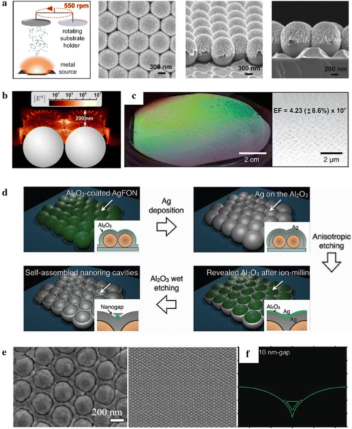
Hot-spot generation using a colloidal crystal template. a Schematic diagram of the metal deposition method applied to a rotating substrate, and SEM images of the AgFON with a high surface roughness. b Calculated electric field intensity distributions near the AgFON substrate coated with a 200 nm silver film. c Uniformity of the nanopatterns at the wafer scale, and tilted SEM image of the AgFON film, showing its high degree of uniformity. d Schematic diagram of the procedure used to fabricate 10 nm metallic nanogaps from nanoring cavities. e SEM image of a FON substrate prepared with 10 nm nanogaps. f Calculated electric field intensity distributions near the FONs prepared with 10 nm nanogaps.
a–c Reproduced with permission from Ref. [39], © 2013, American Chemical Society. d–f Reproduced with permission from Ref. [40], © 2013, John Wiley and Sons