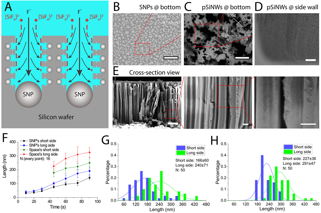
Figure 2.
Synthesis and characterization of pSiNWs. (A) Sketch of synthesizing pSiNWs showing larger SNPs defining the inter-wire spacing between silicon nanowires and tiny SNPs generating porous structures on individual silicon nanowire. Black solid arrows indicate reactant fluoride ions coming to the surface. Red dash lines indicate product silicon hexafluoriode anions leaving the surface into the bulk. (B) Scanning Electron Microscope (SEM) of SNPs formed on the bottom of the channel (bar: 500 nm, insert bar: 200 nm). (C) SEM images of pSiNWs on channel bottom (scale bars: 500 nm, 200 nm for the inset). (D) SEM images of pSiNWs formed on the channel sidewall (scale bar: 2 µm). (E) SEM images of cross-section view of the pSiNWs (scale bars: 2 µm, 500 nm for the two insets). (F) Sizes of SNPs and inter-wire spacing of pSiNWs forests versus the SNP deposition time. (G) & (H) Distribution of the inter-wire spacing of pSiNWs with silver nanoparticle deposition time of 45 s (G) and 60 s (H), respectively.

