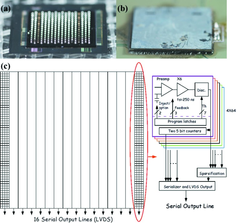
Figure 1.
Images of the VIPIC + sensor die. (a) After deposition of solder bumps onto the back of an ASIC. (b) After flip-chip bonding of VIPIC + sensor to the PCB. (c) VIPIC organization. The dashed line in the box on the right-hand side indicates the split between the different CMOS layers. The prototype is a matrix of 64 × 64 pixels, which are divided into 16 groups. Each group has one serializer and low-voltage differential signaling (LVDS) driver that allows outputting the data from the group.

