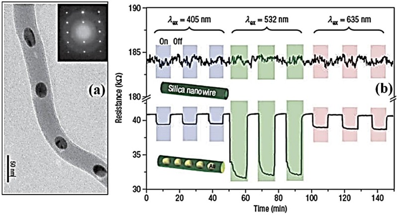
Figure 19.
(a) TEM images showing the structure of metal nanoparticle-encapsulated silicon dioxide nanowire. The inset in in (a) shows an electron-diffraction pattern recorded along the [120] zone axis; (b) Photoresponse measurements. The room-temperature resistance response as a function of time to light illumination for plain silica nanowires (upper part) and gold nanopeapodded silica nanowires (lower part). Shaded (pink, excitation wavelength lex = 635 nm; green, lex = 532 nm; purple, lex = 405 nm) and unshaded regions mark the light-on and light-off periods. Reproduced with permission from [145]. Copyright Nature Publishing Group, 2006.

