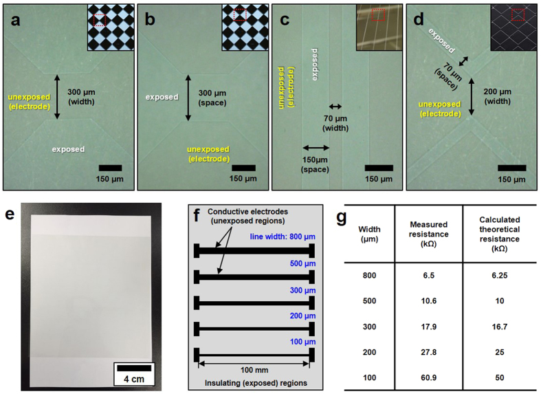
Figure 4.
(a–d) The optical microscopy images of the patterned layer. The inset of each image is a picture of the mask pattern. (e) The picture of the patterned transparent electrode film with dimensions of 200 mm*200 mm. (f) The test patterns of bar-type electrodes with different electrode widths. (g) The measured electrical resistance and the calculated resistance of each bar-type electrode with different widths shown in (f).

