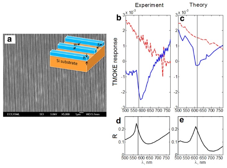
Figure 3.
(a) Scanning electron micrograph and schematic of the Permalloy grating (one-dimensional magnonic crystal). The total area of the grating is 0.5 × 0.5 cm2, h = 100 nm, w = 264 nm, and s = 113 nm. The thickness of the Si substrate is 0.8 mm; (b) Measured and (c) Simulated TMOKE response of the 100 nm-thick reference Permalloy film (dashed line) and Permalloy grating (solid line); Measured (d) and (e) Simulated reflectivity spectra of the Permalloy grating. The vertical straight solid line denotes the Fano resonance wavelengths. Reproduced from [57] with permission by AIP Publishing LLC, Copyright 2013.

