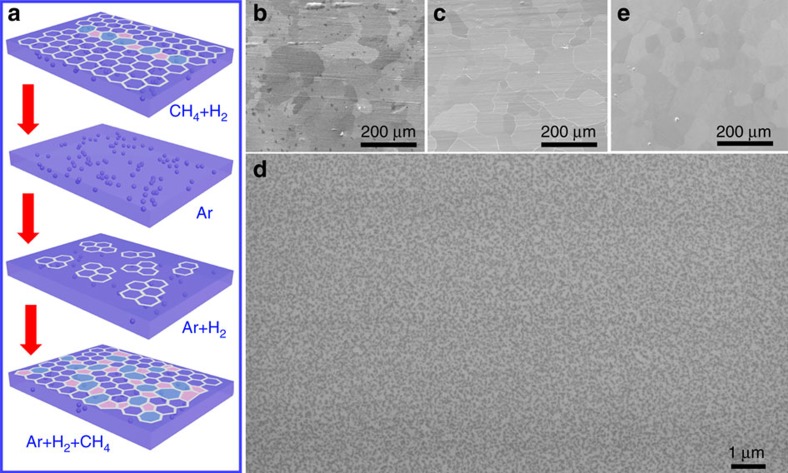
Figure 1. SACVD growth of polycrystalline graphene films with well-controlled grain sizes.
(a) Schematic for the fabrication process of a polycrystalline graphene film. (b) Scanning electron microscope (SEM) image of a graphene film, mostly monolayer, grown on Pt with a mixture of hydrogen (700 standard-state cubic centimetre per minute, sccm) and methane (7 sccm) for 10 min. (c) SEM image of the Pt substrate in b after treating with pure argon (700 sccm) for 20 min, showing that the graphene film has disappeared. (d) SEM image of the Pt substrate in c after treating with a trace of hydrogen (5 sccm) for 20 min, showing that many small graphene domains have appeared. (e) SEM image of a monolayer polycrystalline graphene film formed from d by introducing a low flow rate of methane (0.1 sccm) for 1 h. The reaction temperature was all 900 °C in above cases.

