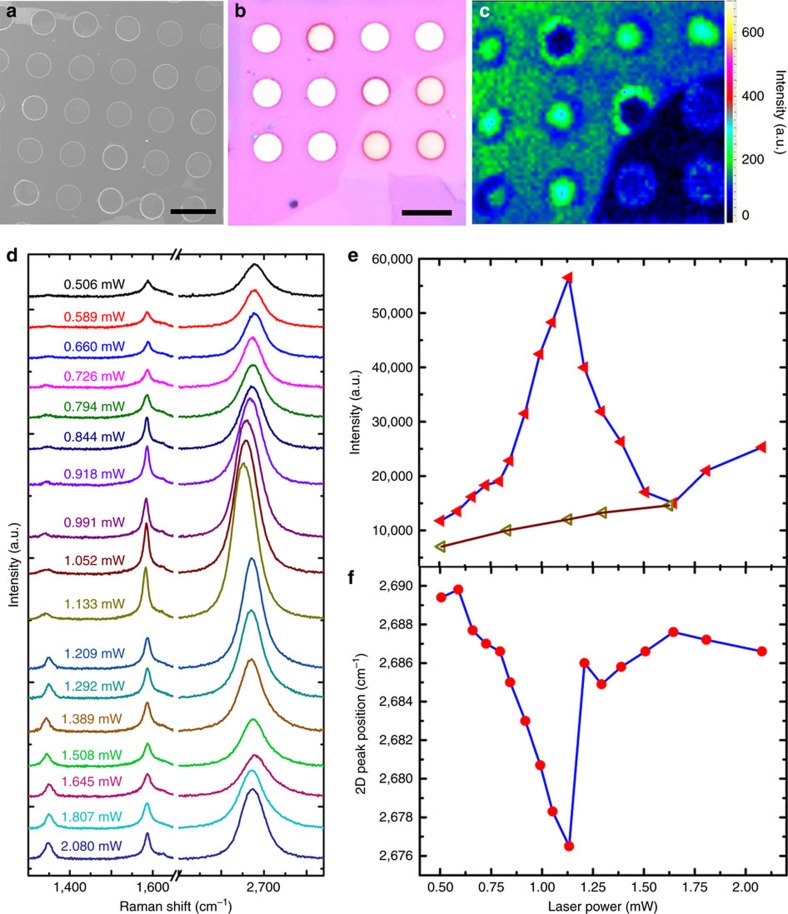
Figure 3. Thermal transport of graphene films with ∼200 nm-sized grains.
(a) SEM image of a polycrystalline graphene film on a holey SiO2/Si substrate. Scale bar, 10 μm. (b) Optical image of a polycrystalline graphene film transferred onto a holey SiO2/Si substrate. Scale bar, 10 μm. (c) Raman map of the polycrystalline graphene film shown in b, and the typical Raman spectra are shown in Supplementary Fig. 12. (d) Raman spectra of the polycrystalline graphene film excited with different power lasers. (e,f) Intensity (e) and position (f) of the 2D peak as a function of laser power.

