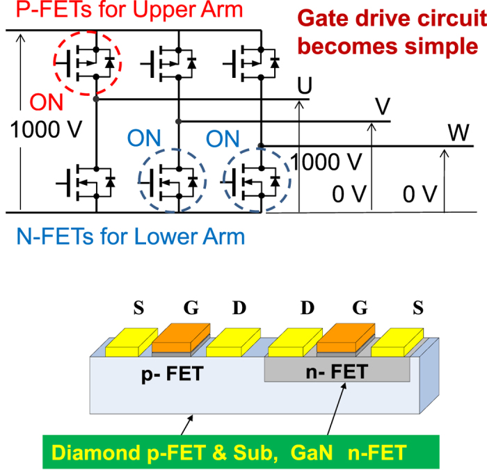
Figure 1. System of complementary wide bandgap semiconductor devices such as that used for power inverters, where the source potentials of the n-channel FETs in the lower arm and the p-channel FETs in the upper arm are fixed at ground level and at a high level, respectively.

This is an almost ideal circuit and is much simpler than that used in current inverter circuits, in which n-channel FETs are used in both the upper and lower arms, and the source potential in the upper arm is not fixed and thus must be changed by on-off switching. An extra gate drive circuit is needed in the current inverter circuit to apply the appropriate gate-source voltage, but is not required in the complementary system shown.
