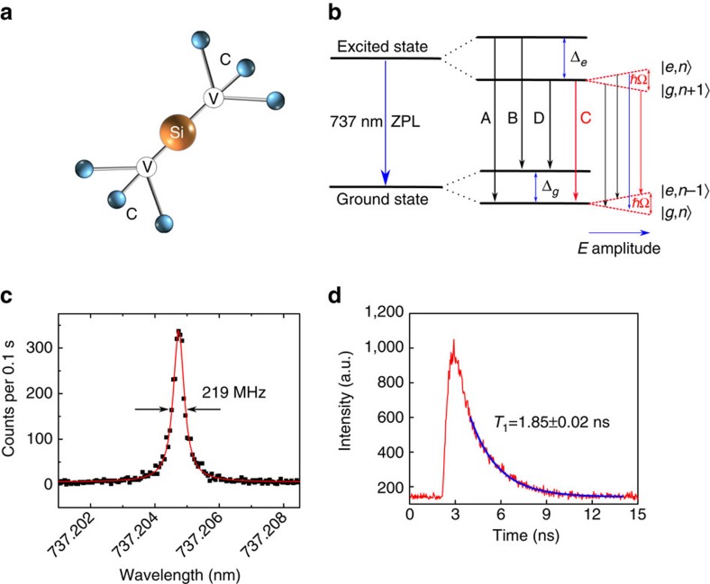
Figure 1. The SiV defect.
(a) Atomic structure of a SiV colour centre in diamond. A silicon atom (yellow) is neighbouring two carbon vacancies (labelled V) in a diamond lattice. (b) Mollow triplet and SiV energy level scheme. The ZPL is at 737 nm. The excited and ground states split by an energy Δe=410 GHz and Δg=228 GHz, respectively, resulting in four transitions labelled as A, B, C and D. With increasing electric field (red) coupling to C transition with a resonant laser, four dressed states are formed and labelled as |g,n〉, |e,n−1〉, |g,n+1〉 and |e,n〉. As the E amplitude increases, the splitting of the dressed states (ħΩ) also becomes larger. (c) Resonant measurement of the C transition linewidth at saturation power, the raw data (black) are fitted by Lorentzian function (red). (d) Lifetime measurement. A resonant laser pulse of ∼100 ps is used to excite the C transition, resulting in a decay (red) of the emitted photons in the time domain, a lifetime of 1.85 ns is extracted from an exponential fitting (blue).

