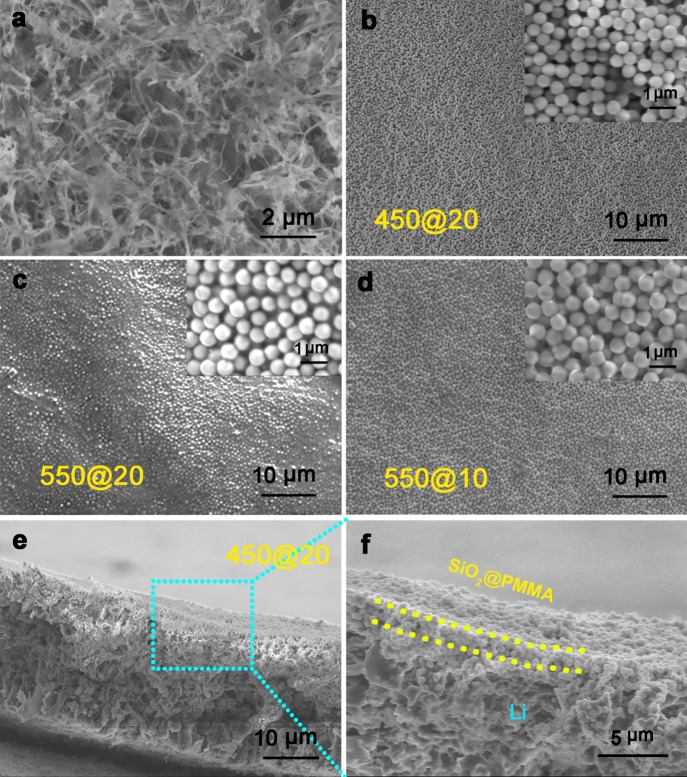
Figure 3.
Li deposition on Cu substrate with and without protective layer of SiO2@PMMA nanospheres. (a) Top-view SEM image of deposited Li metal on bare Cu substrate. (b–d) Top-view SEM images of the 10th lithium deposition on Cu substrate with interfacial layer of SiO2@PMMA nanosphere of (b) 450@20, (c) 550@20, and (d) 550@10 nm at current rate of 1.0 mA cm–2. (e, f) Cross-sectional SEM images of the 10th lithium deposition on Cu substrate with interfacial layer of SiO2@PMMA nanospheres of 450@20 nm.

