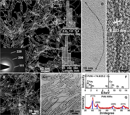
Fig. 2. Morphology and structure characterizations of subnanometer PtNi NWs.

Representative (A and B) STEM and (C) TEM images of subnanometer PtNi NWs. (D) TEM and (E) HRTEM images of two PtNi NWs. (F) TEM-EDS spectrum and (G) PXRD pattern of subnanometer PtNi NWs. The standard diffraction (Pt, JCPDS no. 04-0802) is drawn using blue lines in (G). Left inset of (A) shows SAED pattern of subnanometer PtNi NWs. Right inset of (A) shows the histograms on the diameter and length of subnanometer PtNi NWs.
