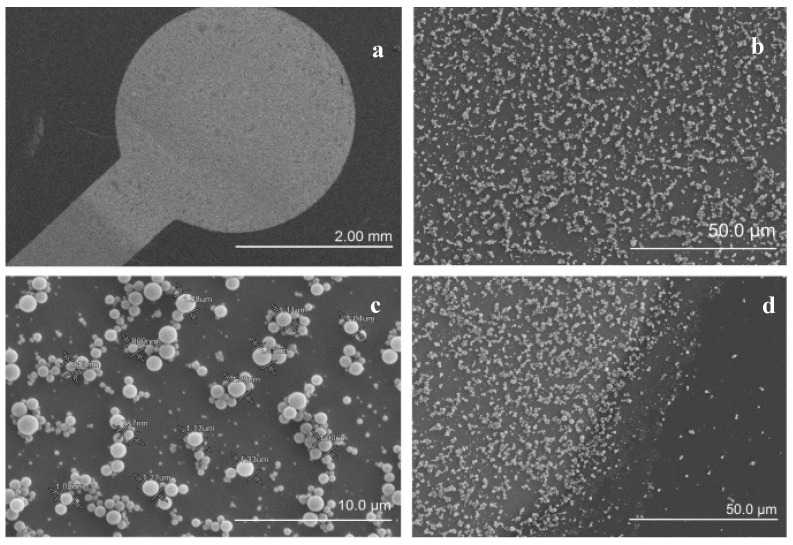
Figure 3.
Scanning electron microscope (SEM) pictures of the electrode surface after functionalization with imprinted polymers. From left to right, top to bottom: (a) SEM picture of electrode surface; (b,c) SEM pictures of centre of the electrode; and (d) SEM picture of the border between the gold layer and wafer. (Reproduced from Reference [23] with permission).

