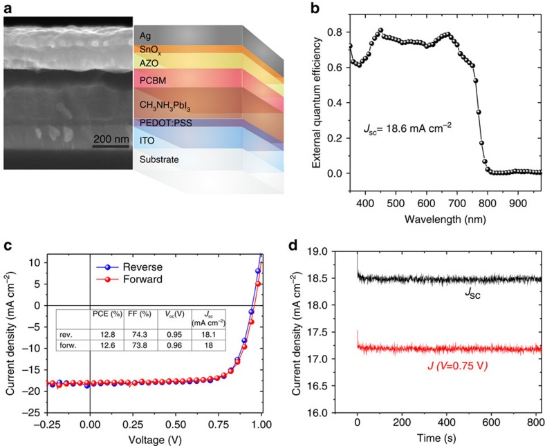
Figure 1. Basic device characteristics.
Scanning electron microscopy (SEM) image of the device cross-section along with the assignment of the respective layers (a). In some devices, the SnOx or the AZO layer has been omitted. Note that the contrast between the AZO and the SnOx layers in SEM is relatively poor. External quantum efficiency (EQE) of a representative device based on AZO/SnOx (b). J/V characteristics measured in forward and reverse direction (c), and current density versus time under 0 V (black) and 0.75 V (red) bias (d).

