
Figure 1.
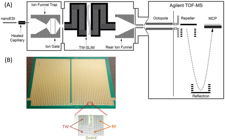
(A) Schematic diagram of the TW SLIM/MS arrangement used in this work. (B) Photo of one of the two TW SLIM surfaces showing the electrodes arrangement with all turns and illustration of a “U” turn (inset) showing the RF, traveling wave, and guard electrodes.