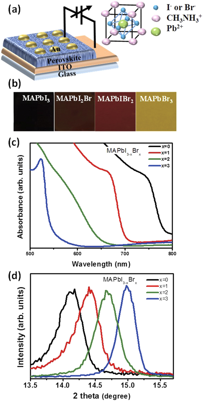
Figure 1. Hybrid organic-inorganic perovskite resistive switching memory devices.

(a) Schematic diagram of memory device with a structure of Au (top electrode)/hybrid perovskite layer/ITO (bottom electrode)/glass substrate. (Right figure: schematic perovskite structure). (b) Photographs of CH3NH3PbI3−xBrx films. (c) UV-vis absorption spectra of CH3NH3PbI3−xBrx films. (d) X-ray diffraction pattern of hybrid perovskite layer with different Br− ion contents to show shift of (110) peaks.
