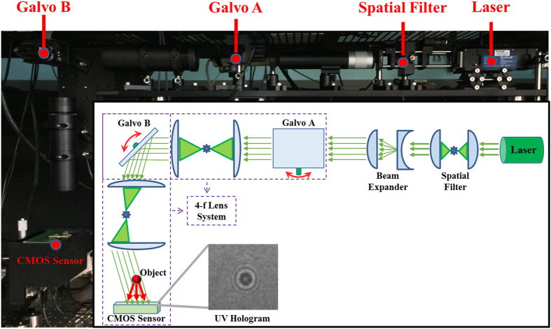
Figure 1. The holographic on-chip imaging platform operating at 266 nm illumination wavelength.
The laser beam is first spatially filtered and then expanded to cover the full CMOS imager active area. The object is directly placed on top of the image sensor, which records in-line holograms of the object across an imaging FOV of >16 mm2. A pair of scanning galvo mirrors controls the angle of incidence to shift the holograms across the image sensor active area, while a pair of 4-f lens systems helps to keep the beam fixed on the sample plane. Note that that there are no imaging lenses between the sample and the image sensor chip, which are separated from each other by ≤0.5 mm.

