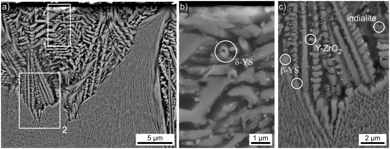
Figure 8. SEM-micrographs obtained from the surface crystallized layer in a cross section after crystallization at 950 °C for 5 h, cooling to RT and then annealing another 1 h at 1060 °C.
EBSD-patterns indexable as the respectively stated phases were obtained from the circled growth structures. (a) Overview of layer 1 and the boundary to layer 2, the framed areas 1 and 2 are presented in greater detail to the right. (b) Detailed SEM-micrograph of the cross section near the edge to the initial surface (top). (c) Detailed SEM-micrograph of the boundary between layer 1 and layer 2.

