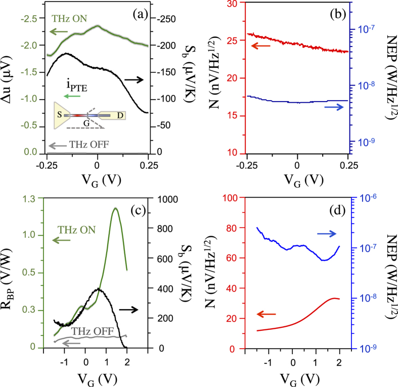
Figure 6. Aperture-coupled THz FET nano-detector response as a function of gate voltage.
(a) left vertical axis: photovoltage ΔuSD (THz beam on) and noise voltage (THz beam off) of sample A plotted as a function of the gate voltage VG. Inset: schematics of the gated NW FET channel and thermoelectric (PTE) current direction; right vertical axis: Seebeck coefficients determined from the theoretical Mott equation; (b) Johnson–Nyquist noise (left) and noise equivalent power (right) of sample A plotted as a function of the gate bias; (c) left vertical axis: Responsivity (THz beam on) and noise voltage (THz beam off) of sample B plotted as a function of the gate voltage VG. Right vertical axis: Seebeck coefficients; (d) Johnson–Nyquist noise (left) and noise equivalent power (right) of sample B plotted as a function of the gate bias.

