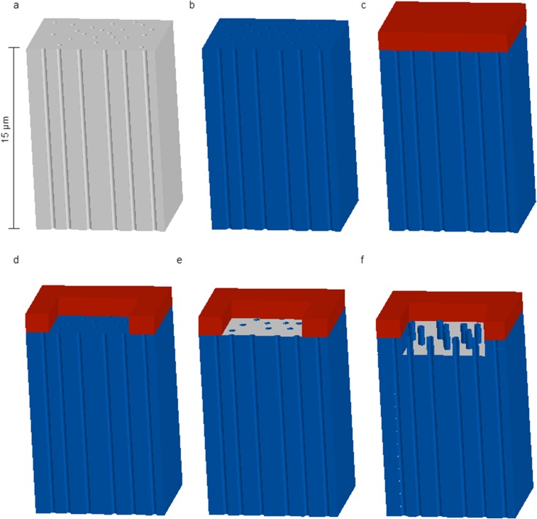
Fig. S1.
Patterned NS platform fabrication workflow. (A) Patterned NS platforms were fabricated starting with track-etched polycarbonate membranes with 150-nm-diameter pores and a pore density of 1 × 10⁸ pores/cm2 (GVS). (B) A 10-nm film of aluminum oxide was coated on all the nanoporous surface of the polycarbonate membranes by Savannah ALD (Cambridge Nanotech) using trimethyl aluminum and water as precursors. A pulse form of a-b-c was used for deposition, where a is the precursor exposure time (0.025 s), b is time for the precursor to remain in the ALD chamber (30 s), and c is the N2 purge time (30 s). (C) A 5-µm-thick positive photoresist film (MEGAPOSIT SPR2203 i-Line photoresist) was spin coated on the top surface of the ALD-coated polycarbonate membrane using a spinning speed of 3,500 rpm for 60 s. The photoresist-coated membrane was baked at 95 °C for 2 min to evaporate resist solvent. (D) The photoresist-coated membrane was exposed to a square pattern of intense UV light for 5 s and then was developed by immersion into the developer (MF-26A) for 60 s. These two steps create the sampling region. (E) After photolithography, the aluminum oxide surface in the microwell was etched away by Plasma Quest RIE with a fast flow composition of 40 sccm BCl3, 30 sccm Cl2, and 5 sccm Ar at 300 W at room temperature, leaving a polycarbonate surface inside the microwell. During the RIE, the unexposed photoresist served as a protection layer. Because the photoresist is much thicker than the alumina layer, the alumina layer inside the microwell can be fully removed without affecting the overall structure of microwells. (F) Oxygen RIE with 30 sccm O2 at 300 W was used to etch the polymer selectively until the desirable NS height was obtained. The etching rate of alumina from oxygen RIE is slower than the etching rate of the polymer; thus the etching of alumina is negligible. On the other hand, the etching rates of the photoresist and polycarbonate are almost the same, so to make NS 1 µm tall, 1 µm of photoresist also will be etched way. The photoresist was thick enough to allow the fabrication of 3-µm nanostraws inside the microwell without completely removing the photoresist during etching. Thus, the photoresist can still act as the blocking layer to cover the pores outside the microwell.

