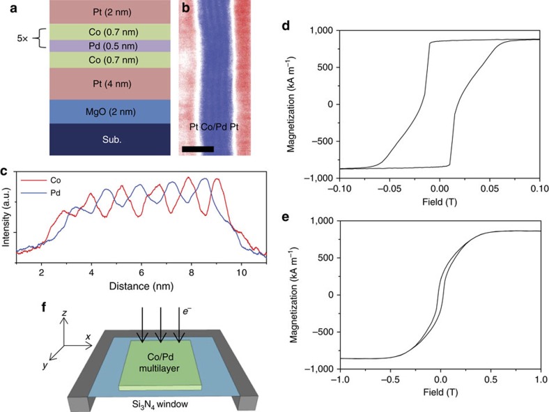
Figure 2. Sample geometry and bulk magnetic properties.
(a) Schematic and (b) scanning TEM (STEM) high-angle annular dark field image of the thin film structure studied in this work. Scale bar, 5 nm. (c) EELS line scan showing the location of distinct Co and Pd layers. (d) Out-of-plane and (e) in-plane VSM hysteresis measurements of the film shown in a, grown on a thermally oxidized Si wafer. The sloped reversal in d is indicative of domain mediated reversal. (f) Experiment geometry for L-TEM imaging. The Si3N4 window is 0.5 μm × 0.5 μm and 100 nm thick.

