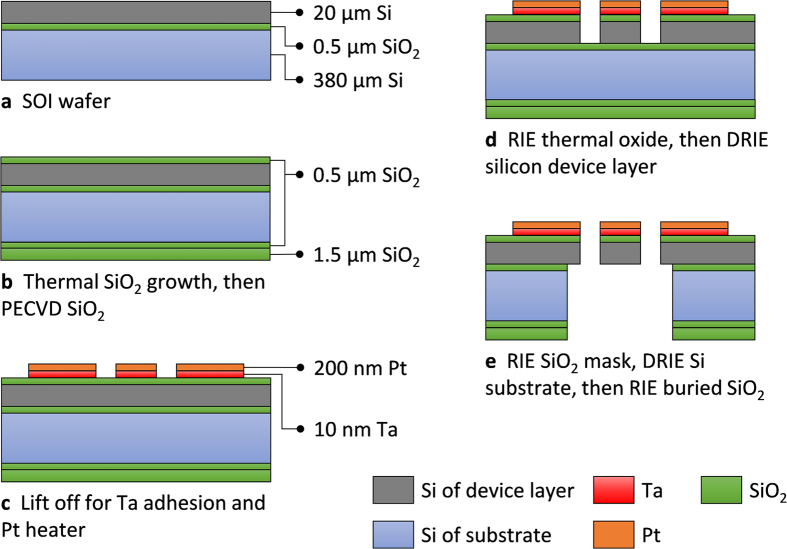
Figure 4. Fabrication steps of the Near-field NanoThermoMechanical rectifier (drawings are not to-scale).
(a) Plain SOI wafer with a 20-μm thick device layer, and 0.5-μm buried silicon dioxide layer. (b) Thermal growth of 0.5-μm silicon dioxide layer, and plasma enhanced chemical vapor deposition of 1.5 μm of silicon dioxide. (c) Platinum microheater patterning with tantalum adhesion layer. (d) Reactive ion etching the (RIE) thermal silicon dioxide layer and then deep reactive ion etching (DRIE) of the silicon device layer to form the microdevice structure. (e) Etching of the backside of the substrate to release the microdevice structure.

