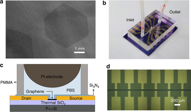
Figure 1. Photos and layout of the sensor chip.
(a) Scanning electron microscope (SEM) images of graphene single-crystal domain. (b) Photograph of the sensor composed of multi-G-FETs with a microfluidic channel along with solution inlet and outlet as labelled. (c) Cross-sectional view of an individual G-FET device. (d) Optical micrograph of the sensor with multi-G-FET detecting channels.

