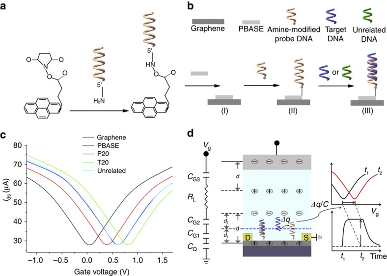
Figure 2. Functionalization and properties of G-FETs.
(a) Molecular geometry of PBASE and its link to the probe DNA. (b) Functionalization of graphene surface by PBASE, immobilization of a probe DNA (in orange) by reacting with the PBASE and hybridization of the probe DNA with target (in blue) and unrelated, control DNAs (in green). (c) Source drain current at a constant source drain voltage (0.1 V) with varying gate voltage for the bare graphene (in black) and after each addition of the following reagents in sequence, 10 mM PBASE (in red), 100 nM probe DNA P20 (in blue), 5 nM complementary DNA T20 (in green) and 5 nM unrelated, control DNA U20 (in cyan, essentially indistinguishable from the blue curve). (d) A schematic diagram of the sensing model of a G-FET together with the equivalent circuit with four parallel plate capacitors (CG1, CG2, CG3 and CQ) and a resistance (RL) connected in series. CG1, CG2 and CG3 denote the capacitance between graphene and solution, the capacitance of the DNA to solution and the capacitance between Pt gate and solution, respectively. CQ denotes the quantum capacitance of graphene associated with the finite density of states due to Pauli principle. RL is the electrical resistance of the ionic solution. When target DNAs dock on the graphene surface, a transfer curve shift (ΔVcnp) occurs due to changes of charges near the graphene sensor chip surface that is continuously monitored.

