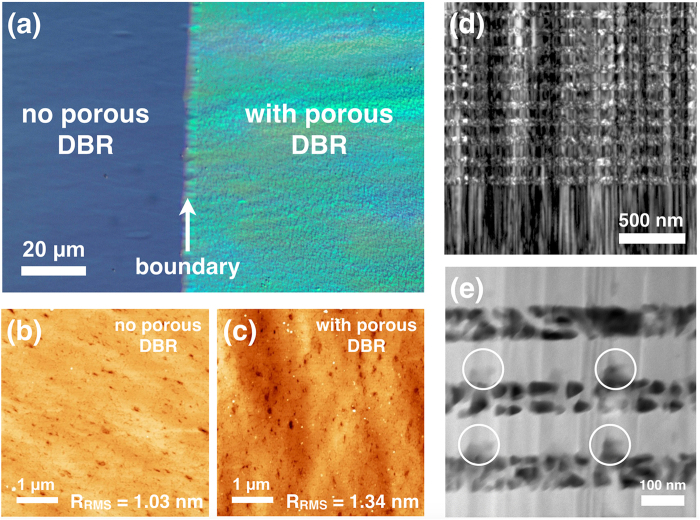
Figure 2.
(a) A top-view Nomarski optical image of the GaN/MP-GaN DBR sample, where a darker non-porous region and highly reflective porous region can be seen (the boundary is marked by the white arrow). AFM images taken from regions (b) without porous DBR and (c) with porous DBR. (d) Weak-beam dark-field TEM image taken along [0001] using g = 11–20. (e) HAADF-STEM image of the MP-GaN DBR structure. The white circles indicate the positions where the NID-GaN layers have also been etched due to the vertical etching component of the EC porosification process.

