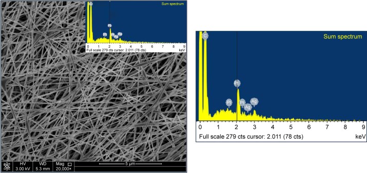
Figure 1.
SEM image of fabricated electrospun mat.
Notes: SEM image at 20,000× of electrospun nanofibers of PVA/chitosan/AgNPs blends of 12 wt%/0.6 wt%/0.9 wt%, respectively, using the following electrospinning conditions of 10 cm, 18 kV, and 0.3 mL/h. The EDS was collected on the PVA/chitosan/AgNPs.
Abbreviations: SEM, scanning electron microscopy; PVA, poly(vinyl alcohol); AgNPs, silver nanoparticles; EDS, energy dispersive spectrum; wt, weight; HV, high voltage; Mag, magnification; WD, working distance.

