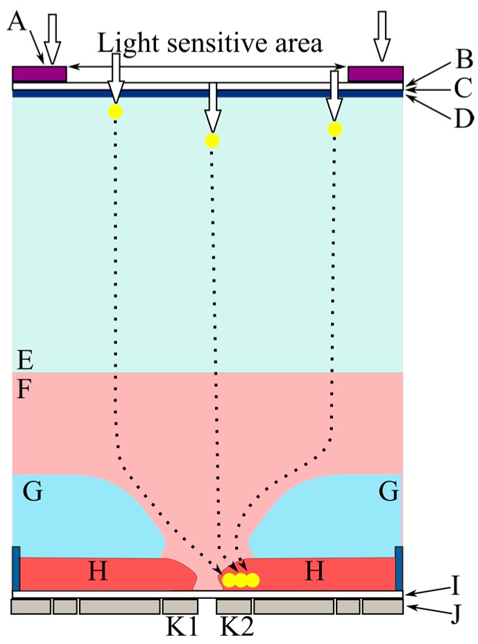
Figure 2.
A cross-section structure of a pixel of a backside-illuminated (BSI) image sensor and trajectories of signal electrons. A: light shield; B: oxide; C: interface between the backside oxide layer and the silicon layer; D: backside hole accumulation layer; E: p− layer, F: n− layer; G: p-well; H: memory and circuit areas; I: oxide; J: electrodes and wires; K: collection gates.

