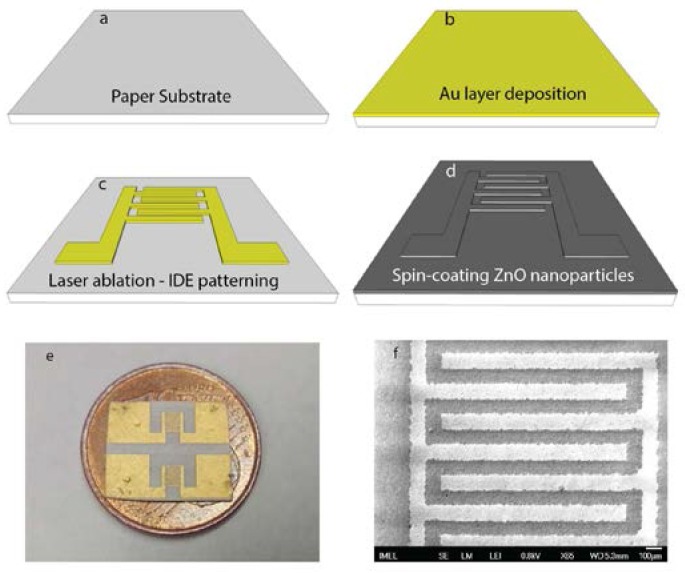
Figure 1.
Microdevice fabrication process. (a) Paper substrate, (b) Deposition of Au layer, (c) Laser micromachining of the interdigitated electrodes, (d) Spin-coating the ZnO-nanoparticle layers, (e) Photograph of the finished fabricated devices on paper (2 devices on a coin of 1 cent), (f) Scanning Electron Microscope (SEM) image of the resulting nanotextured ZnO film.

