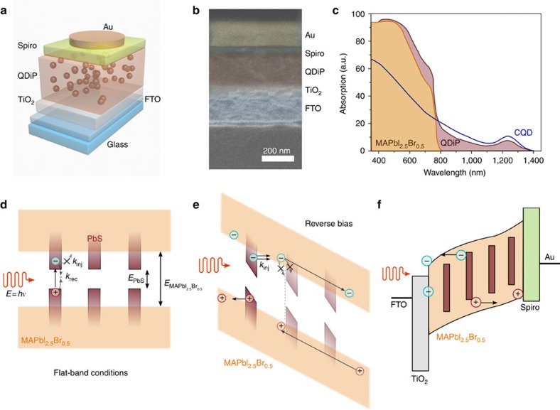
Figure 1. Field-emission QDiP photodetector.
(a) Photodiode device schematic. The QDiP photoactive layer is sandwiched between TiO2 (electron-transport layer) and spiro-MeOTAD (hole-transport layer). (b) Cross-sectional SEM of a typical device, color-coded overlay for clarity. (c) Absorption of pure MAPbI2.5Br0.5 perovskite, QDiP (1:1 ratio) and colloidal quantum dot (1 eV) films. Above 800 nm MAPbI2.5Br0.5 is not photosensitive, whereas the QDiP extends up to 1,400 nm. (d) For a type-I heterojunction, at flat band conditions photogenerated charges in the CQD phase cannot escape and lose their energy via recombination. Charges in the perovskite will eventually get trapped and recombine through the quantum dots. (e) Under sufficient reverse bias, carriers can tunnel into the MAPbI2.5Br0.5 host assisted by the high electric field and be collected. The transport matrix needs therefore to combine high mobilities with minimized recombination at the dot's interface in order to repeal recapture probability. (f) Proposed operation of the field-emission QDiP photodiode.

