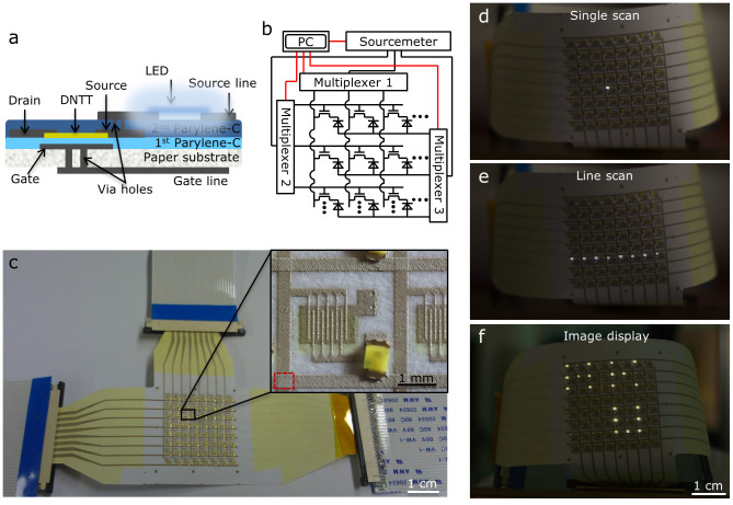
Figure 4. OFET AM driver scanning and information display.
(a) Schematic of OFET AM driver. (b) Array driving circuit, red lines correspond to digital signals and black lines to analog signals. (c) Optical image of OFET AM LED driver, standard connector interfaces to FFCs (flat flexible cables) are formed by screen-printing. Inset is an enlarged single pixel of the array, where the red dotted box indicates the insulation layer (2nd parylene-C) between drain (vertical) and source (horizontal) electrodes. VGS = −40 V and VDS = −15 V are used to operate the OFET AM LED driver. Different operating conditions of the driver are shown. (d) Single scan, one by one operation of each pixel. (e) Line scan, row by row operation of pixels. (f) Image display using programmed fast scanning to display “HKU” in capital letters.

