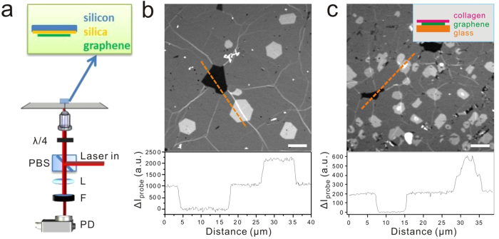
Figure 2. TA imaging of graphene on silicon-based sheet and with collagen coating.
(a) Layout of epi-detection of TA signals. PBS: cube polarization beam splitter installed in interchangeable turret; λ/4: quarter-wave plate; L: lens with 100 mm focal length; F: bandpass filter used before photodiode; PD: large area photodiode. The graphene sheet was prepared on top of a thin silica layer (~300 nm), with silicon sheet underneath. (b) Epi-detected TA imaging of graphene and intensity profile along the dashed line. Single layer, double layers and defects were clearly resolved in a quantitative manner. The average power used for pump beam was 5 mW at 665 nm, and 10 mW for probe beam at 820 nm. Scale bar: 10 μm. (c) TA imaging of graphene with collagen coating and intensity profile along the dashed line. Inset: diagram of the sample preparation. Graphene sheet was placed on a glass coverslip with 0.17 mm thickness, and collagen was coated on top of the graphene sheet. Scale bar: 10 μm.

