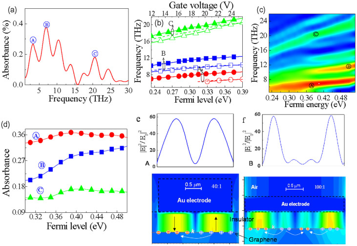
Figure 2. The plasma wave resonance in monolayer and double-layer FETs with grating coupler (Fig. 1(c)), period Λ = 2.8 μm, gate length L = 2.4 μm (corresponding to the filling factor f = 0.86), the thickness of dielectric tunneling junction d = 50 nm.
(a) All kinds of resonances have higher Q value than other conventional 2DEG system like GaN. (b) The shift of plasma wave resonance frequency after electrically tuning the Fermi level, solid symbols indicate the frequency dependence of plasma waves in double-layer FETs on the gate voltage, and the dashed line is that of monolayer FETs, both of these device exhibit approximately Vg1/4 relationship. Open symbols is the frequency dependence of plasma waves in monolayer FETs on Fermi level relative to the CNP. (c) and (d) are the contour map of plasma wave resonance in monolayer FETs. It is found that there is the non-monotonous dependence of resonance on Fermi level. (e)The near-field enhancement caused by the screening of the electrodes is related to the first two resonances A and B.

