Fig. 4.

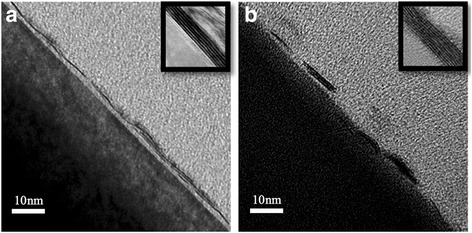
High-resolution transmission electron microscopy cross section images of WS2 (d WO3 = 1 nm) grown on a Al2O3 and b SiO2 substrates. Insets show corresponding image for the thick WS2 (d WO3 = 8 nm)

High-resolution transmission electron microscopy cross section images of WS2 (d WO3 = 1 nm) grown on a Al2O3 and b SiO2 substrates. Insets show corresponding image for the thick WS2 (d WO3 = 8 nm)