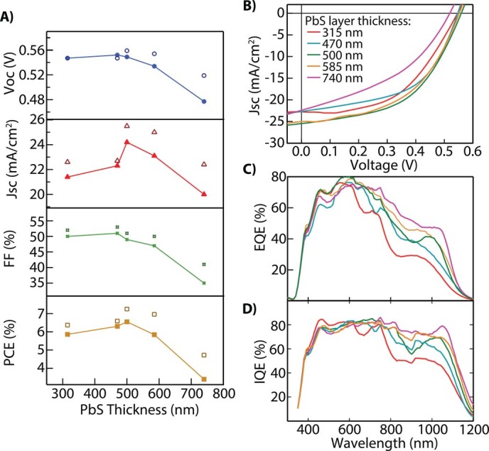
Figure 4.

A) VOC, JSC, FF, and PCE plotted as a function of device thickness for spincoated PbI2-treated devices. Solid symbols represent the average of 6 devices and hollow symbols are the best devices. B) J-V curves of cells shown in panel A with the best cell reaching a PCE of 7.25% with 500 nm thickness of the QD layer. C) EQE response of cells showing improved response of longer wavelength light as the cell absorbs more light. D) Internal quantum efficiency (IQE) determined by dividing the EQE by the absorption. The color coding is consistent in panels B-D and annotated in the legend of panel B.
