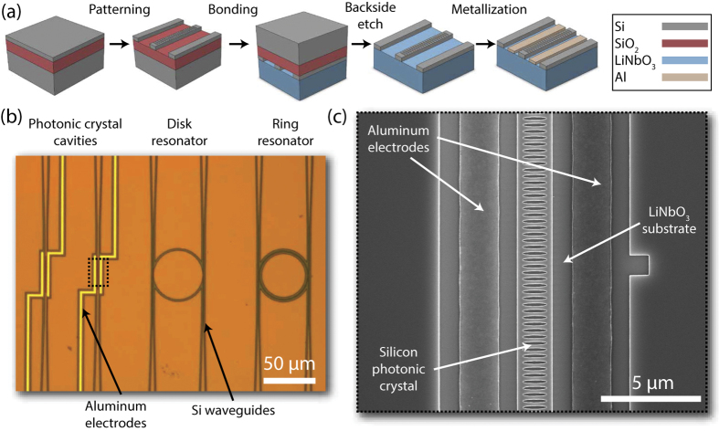
Figure 1. Fabrication of SiLN electro-optic devices.
(a) The SiLN fabrication process, showing e-beam lithography and etching of photonic structures into an SOI die, bonding to LN, removing the backside silicon, and patterning electrodes. (b) An optical microscope image showing fabricated ring, disk and photonic crystal structures. (c) A scanning electron micrograph image of a SiLN photonic crystal with electrodes.

