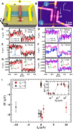
Fig. 1. Detection of current (Id)–independent spin signal in a Bi2Te2Se (BTS221) thin flake by spin potentiometry.

(A) Schematic 3D device structure used in the potentiometric measurement, showing a three-terminal electrical connection. The TI surface defines the x-y plane, and the surface normal defines the z direction. The two outside nonmagnetic (for example, Au) contacts (the left is grounded) are used to inject a DC bias current, and the middle FM (for example, Py) contact is magnetized by an in-plane magnetic B field (labeled) along its easy axis (y direction, with −y defining the positive B and M direction). The middle FM contact is a tunneling probe (with a thin Al2O3 tunnel barrier underneath in our devices). (B) Optical image of device A used in the potentiometric measurement. (C to H) Voltage measured by the FM spin detector (Py) on device A as a function of in-plane magnetic field for representative bias currents (Id) of 100 pA (C), −100 pA (D), 10 nA (E), −10 nA (F), 1 μA (G), and −1 μA (H). The directions of Id (red arrow), the inferred channel (top surface) spin polarization S (dashed green arrow), and Py magnetization M (black arrow) are labeled in (G) and (H). (I) The voltage change δV = V+M − V−M [marked by the arrow in (E) and defined as the spin signal indicating the presence of channel spin polarization] as a function of the applied DC bias current. Here, δV is extracted from forward sweep traces (backward sweeps yield similar results). All the measurements were performed at the temperature T = 0.3 K.
