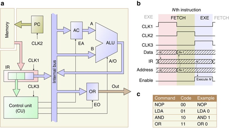
Figure 1. Microprocessor architecture.
(a) Block diagram, showing the arithmetic logic unit (ALU) with inputs A and B, accumulator (AC), control unit (CU), instruction register (IR), output register (OR) and program counter (PC). Enable signals (EA and EO) and operation selection code (A/O) are supplied by the CU to the respective subunits. CLK signal generation and memory are implemented off-chip. (b) Timing diagram for the Nth instruction cycle. During the FETCH sequence the content of the memory is loaded into the IR and the address, stored in the PC, is increased. During the EXE sequence the command, stored in the IR, is executed. (c) Instruction set of the microprocessor. NOP is the no-operation instruction; LDA transfers data from the memory into the AC; AND and OR perform logical operations.

