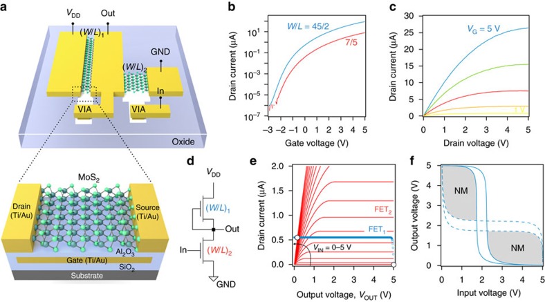
Figure 2. Characterization of MoS2 transistors and inverter.
(a) Schematic drawing of an inverter circuit (top) and an individual MoS2 transistor (bottom) in gate-first technology (see Supplementary Fig. 5 for corresponding micrograph). (b) Transfer characteristics of load (W/L=45/2) and pull-down (W/L=7/5) transistors. (c) Output characteristic for gate voltages between 1 and 5 V (in 1 V steps). (d) NMOS inverter circuit schematic. (e) Graphical construction to determine the output voltage VOUT of an inverter for a given input voltage VIN. The blue symbols show the load curve and the red lines are the output characteristics of the pull-down transistor (in 0.25 V steps). The intersection point of both curves determines VOUT. (f) The solid line shows the measured voltage transfer characteristic of an inverter. By mirroring this curve (dashed line) a butterfly plot is obtained, from which NM can be extracted by nesting the largest possible square in the grey shaded area.

