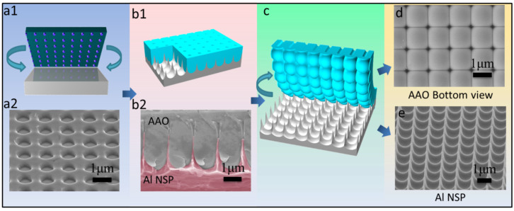
Figure 1. Fabrciation process of 3-D nanospike.
(a1–a2) Schematic diagram of nanoimprint process on flat Al foil with a silicon stamp and SEM image of a imprinted aluminum foil. (b1–b2) Schematic diagram and SEM image of NSP under squarely ordered AAO after anodization (Al NSP is indicated with red false color in b2). (c) Schematic of AAO removal to expose NSP underneath. (d) SEM of bottom view of squarely order AAO. (e) SEM of perfectly ordered Al NSP array.

