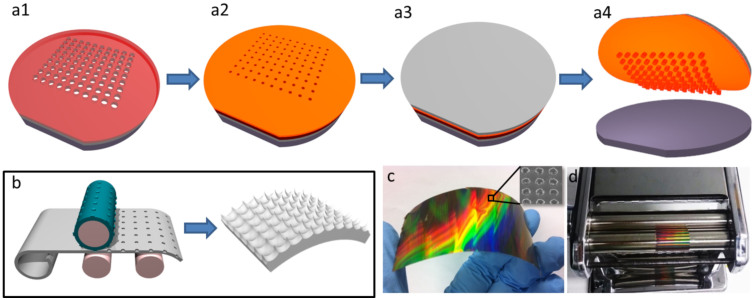
Figure 5. Roll-to-roll fabrication of large scale NSP substrate.
(a1) Silicon wafer patterned with double layers photoresist hole array. (a2) Sputtered Ti/W/Cu on photoresist for seed layer of the subsequent metal electrodeposition. (a3) Thick copper and nickel electrodeposited on the seed layer. (a4) Flexible nanoimprint master foil released in acetone. (b) Schematic of Roll-to-roll nanoimprint to fabricate large scale NSP on flexible Al foil. (c) Thin metal foil of nanoimprint master and inset shows SEM micrograph of its surface. (b) Roll-to-roll nanoimprint set-up with nanoimprint foil master mounted on.

