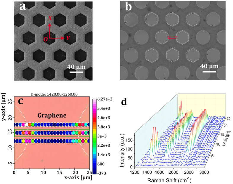
Figure 2. Patterning graphene through a nickel mask by UV ozonation.
SEM topographical images of (a) the nickel mask and (b) graphene microstructures patterned by UV ozonation without any magnetic assistance. White dotted hexagons in (b) represent actual hole positions of the mask. (c) Micro-Raman map of the defect band (D band) intensity in the region denoted by the red rectangle in (b), and (d) its Raman spectrum evolution for the dots outlined by the green rectangle in (c). a.u., arbitrary unit; graphene edges are all denoted by white dotted lines in Raman mapping.

