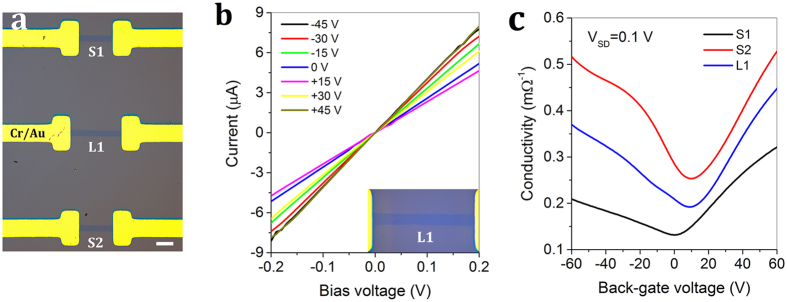
Figure 5. Characterization of the graphene FET array patterned by the vertical magnetic-field-assisted UV ozonation.
(a) Optical image of the graphene FET array consisting of three devices with two different channel lengths. Scale bar, 200 μm. (b) Linear relationship between current and bias voltage for L1 at different back-gate biases ranging from −45 to +45 V in a step of 15 V. The inset shows a zoom-in optical image. (c) Conductivity curve as a function of gate bias for the graphene FET array at a fixed source-drain voltage VSD = 0.1 V.

