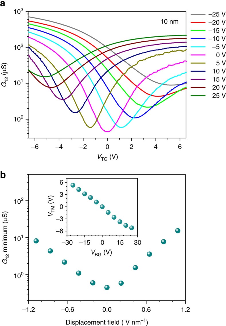
Figure 3. Bandgap tuning in a 10 nm-thick BP film.
(a) The 10 nm-thick BP film conductance as a function of top gate bias (VTG) at different static back gate biases (VBG) from −25 to 25 V. (b) The minimum conductance at the charge-neutrality point as a function of external displacement field. Inset: the top gate bias at which the minimum conductance occurs (VTM) as a function of the back gate bias (VBG).

