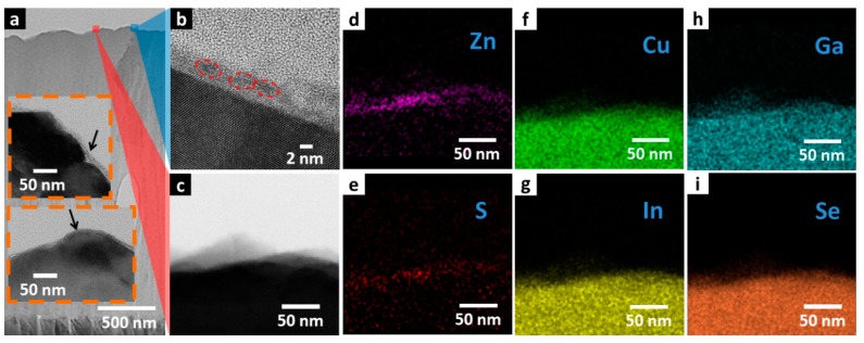
Figure 5.
(a) TEM overview image of CIGS absorber layer capped by the ZnS NPs layer. Insets show magnified view at ZnS NPs/CIGS interface. (b) TEM image of ZnS NPs/CIGS pn junction magnified at individual ZnS NPs (indicated by the blue shade), in which single ZnS NPs are marked by red dashed circles. (c) TEM image of where energy dispersive spectrometer (EDS) mapping is conducted, indicated by the red shade, and EDS mapping of (d) Zn, (e) S, (f) Cu, (g) In, (h) Ga, and (i) Se.

