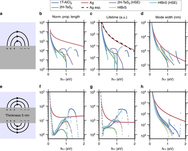
Figure 4. Plasmon waveguiding figures of merit.
The upper panels show the normalized plasmon propagation lengths Re(kp)/Im(kp) (b), lifetimes (c) and mode width (d) for a plasmon on a single interface (a). The lower panels (e–h) show the same results for a 5 nm thin film. The more efficient dielectric screening in silver reduces the fraction of the electric field located within the metal as compared to the case of the vdW metals, resulting in lower losses, longer propagation lengths and lifetimes. On the other hand, since most of the electromagnetic energy is stored in the part of the electric field distributed over the dielectric, the mode widths of the surface plasmon becomes relatively large. Reducing the thickness of the metal to a 5 nm thin film pushes a larger fraction of the electric field into the metal leading to more confined modes. The redistribution of the electric field from dielectric to metal is more significant for silver explaining the overall better performance of the vdW metals for the thin-film geometry. Experimental data for the Ag surface plasmon was adapted from ref. 38.

