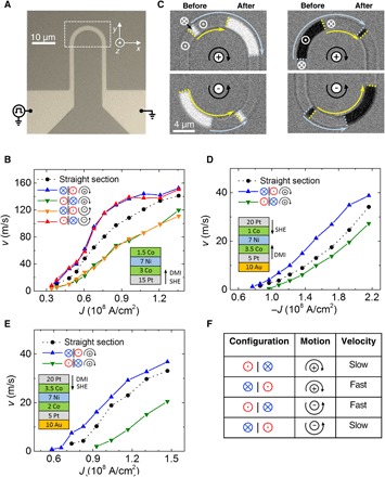
Fig. 1. Dependence of the DW velocity on curvature for different structures.

(A) Optical image of a typical U-shaped device with R = 7 μm and w = 2 μm. (B) v versus J shows faster or slower DW motion in a curved nanowire compared to a straight wire. (C) Representative Kerr images showing the expansion or contraction of a magnetic domain along the positive or negative curvature of a curved nanowire. The Kerr images are taken before and after the application of two 100-ns-long electrical pulses with a current density of 0.6 × 10⁸ A/cm2. They are overlaid together, and the unedited picture is available in fig. S14. The yellow (gray) dots indicate the positions of ⊙ | ⊗ (⊗ | ⊙) DWs, and the arrows represent the trajectory of their motion. (D and E) v versus J showing the same relationship [as (B)] between the sign of the curvature on the increase or decrease in the DW velocity irrespective of the signs of DMI and SHE. (F) Truth table derived on the basis of (B), (D), and (E). Note that thicknesses of the layers in (B), (D), and (E) are in angstrom.
